SND-MPL Polycrystalline Synthetic Micron Diamond Powder: Superabrasive for Scratch-Free Polishing and High-Precision Lapping
Top Introduction
Description
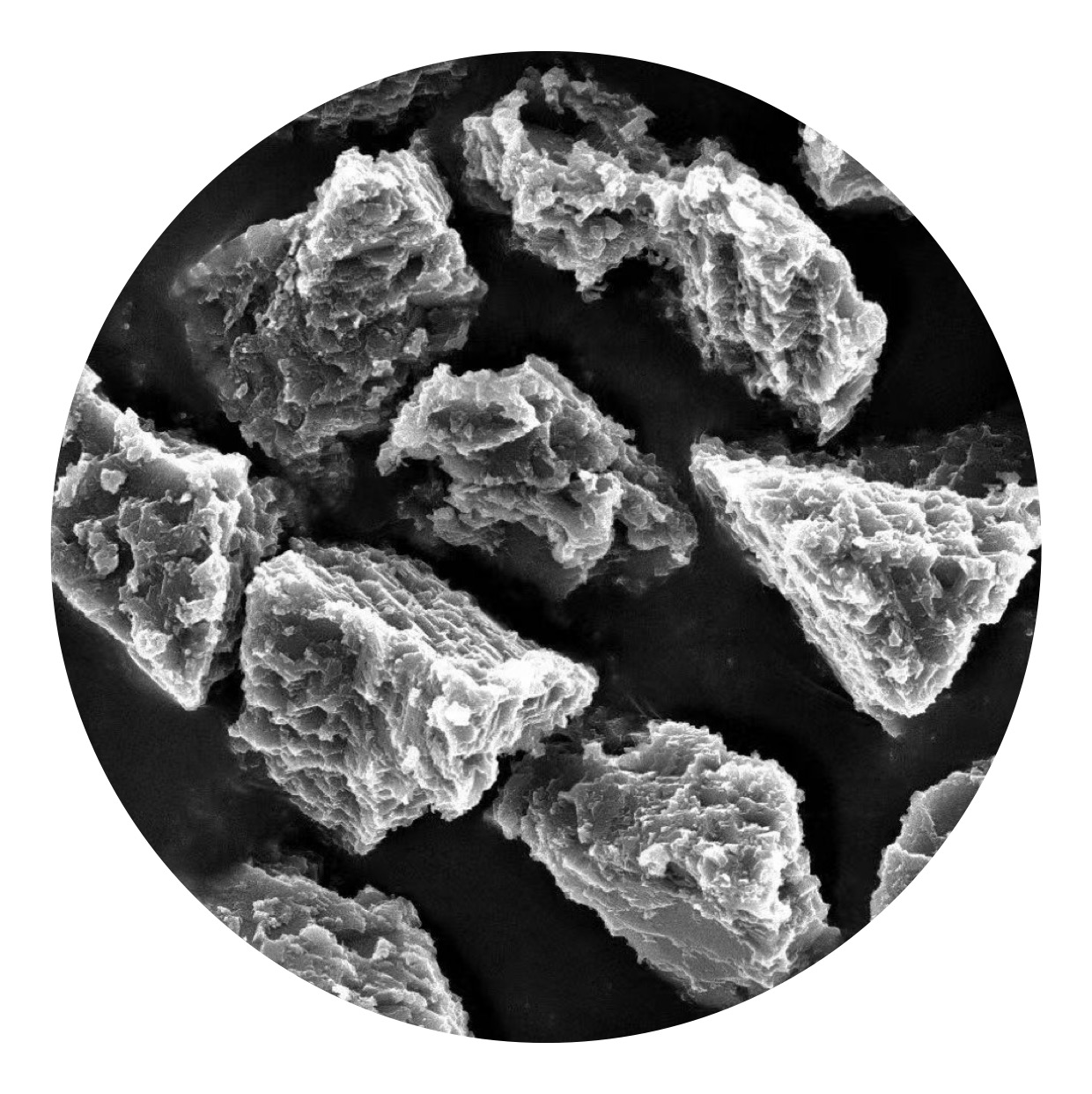
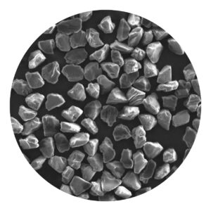
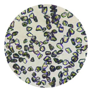
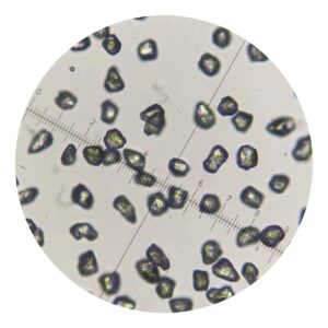
SND-MPL combines the multi-edge cutting dynamics of true polycrystalline diamond with the consistency and affordability of synthetic single-crystal diamond. Each micron particle undergoes controlled chemical etching, forming 5–8 deactivated micro-edges that evenly distribute polishing pressure and prevent deep grooves or surface scratches.
This unique honeycomb morphology allows SND-MPL to remove material gently yet efficiently, producing mirror-grade finishes on optics, watch crystals, sapphire windows, and wafer surfaces. Its textured, micro-rough surface (Ra 0.2μm) improves adhesion in resin or vitrified bond polishing pads, reducing grit loss and extending tool life by up to 50%.
Compared to traditional single-crystal diamond powders, SND-PL provides 2–4× faster polishing speed, zero scratch rate, and superior material yield—making it a top choice for advanced polishing and lapping applications across optics, electronics, and luxury industries.
Technical Edge & Engineering
- Honeycomb Edge Structure: Chemically etched to form 5–8 micro-edges per grain, spreading the polishing load evenly and eliminating deep scratches common with sharp-edged monocrystalline diamonds.
- Toughness Optimization: Thermal conditioning lowers microhardness to HV 6,000–6,500, reducing chipping and improving control during ultra-fine polishing.
- Micro-Rough Surface: Engineered surface roughness of Ra 0.2μm ensures stronger bond retention in resin and vitrified systems—reducing grit shedding by 40%.
- High Purity & Consistency: Produced with narrow PSD tolerance (±5%), ensuring stable surface finishes across large-area polishing and wafer planarization processes.
Key Advantages
- True Scratch-Free Finish: Achieves Ra ≤0.03–0.05μm on optical glass and sapphire lenses with >95% reflectivity—zero secondary polishing required.
- 2–4× Higher Efficiency: Multi-edge microstructure accelerates removal rate while preserving surface integrity, cutting polishing time by up to 70%.
- Cost-Effective Polycrystalline Substitute: Delivers polycrystalline diamond performance at 30% lower cost, ideal for mid-tier optical and electronic polishing applications.
- Extended Tool Life: Enhanced grit bonding extends pad or wheel life by 40–50%, reducing operational costs for high-volume production lines.
- Universal Compatibility: Works seamlessly with resin bond, vitrified bond, and electrostatic-coated polishing pads, adaptable for manual or automated polishing systems.
Core Applications Across Industries
Optical & Electronics
- Optical Glass Polishing: Achieves mirror clarity (Ra ≤0.03μm) on camera lenses, laser optics, AR/VR lenses, and aerospace windows, meeting EN 12150 (EU) and ANSI Z87.1 (NA) optical standards.
- Semiconductor Wafer Lapping: Used for backside polishing of silicon and sapphire wafers, ensuring smooth, defect-free surfaces for chip bonding and packaging.
- Precision Optoelectronic Components: Polishes sapphire LED substrates, quartz lenses, and ceramic optical elements for display and sensor industries.
Gem & Luxury Finishing
- Gemstone Polishing: Enhances brilliance and clarity in diamonds, rubies, sapphires, and emeralds—delivering scratch-free mirror finishes for luxury jewelry.
- Watch & Jewelry Metals: Buffs gold, platinum, and coated metal surfaces (Swiss watch cases, jewelry fittings) without damaging delicate plated layers.
- High-End Artisanal Polishing: Used in Belgian diamond cutting workshops and Swiss luxury brands for achieving ultra-bright luster.
Technical Specifications
| Property | Specification |
|---|---|
| Particle Size Range | 0.5–5μm (fine polishing), 5–15μm (lapping/pre-polishing) |
| Crystal Structure | Polycrystalline-like with honeycomb multi-edges |
| Toughness (HV) | 6,000–6,500 |
| Surface Roughness (Ra) | 0.2μm (textured) |
| Bond Compatibility | Resin, vitrified, electrostatic pads |
| Polishing Efficiency | 2–4× vs. standard micron diamonds |
| Min. Polished Surface Roughness | ≤0.03μm (optical glass, wafers) |
FAQ
Q1: How does SND-MPL prevent scratches compared to traditional micron diamonds?
A: Its honeycomb multi-edge design evenly distributes pressure, preventing the sharp edge gouging typical of regular diamonds. This results in uniform material removal and zero scratch polishing on optical or gem surfaces.
Q2: Can SND-MPL be used for semiconductor wafer lapping?
A: Yes—its 0.5–5μm fine range is ideal for backside wafer polishing with Ra ≤0.03μm. The low-toughness microstructure avoids wafer microcracks or surface contamination.
Q3: How does SND-PL perform in resin-bond polishing pads?
A: Excellent adhesion and low grit shedding make it perfect for resin or vitrified pads—improving pad life by up to 40% and maintaining consistent surface quality across hundreds of cycles.
Q4: What are the best storage conditions?
A: Store in sealed, moisture-proof containers at 15–28°C, <65% humidity. Avoid acids, solvents, or UV exposure to preserve the passivated edge structure for up to 24 months.
SND-MAG Diamond Agglomerated Micron Powder

Avaliações
Não há avaliações ainda.